Analysis of Terminal Materials and Welding Processes
The growth of power semiconductor packaging technology is, to some extent, fueled by breakthroughs in material engineering and production techniques., The industry has pioneered an all-copper processing approach, so as to boost their power cycling endurance and long-term operational stability and alleviate the thermal expansion coefficient mismatch among diverse materials in modules. This methodology fundamentally consists of three key elements: ultrasonic welding of module copper power terminals, copper wire bonding interconnection and chip copper metallization.
Pin ultrasonic welding has been developed as a new connection method, as in specific application scenarios, higher requirements are placed on the reliability of pin connections. Pin ultrasonic welding offers unparalleled advantages in connecting the same metals. Since ultrasonic metal welding does not require flux or external heat sources, the welded structure will have no residual stress and won’t deform because of heat.
Pin ultrasonic welding has gradually gained favor in the market. It has achieved close metallic covalent bonding between identical materials.
Traditional soft soldering may lead to poor pin welding due to factors such as equipment air pressure fluctuations, abnormal reflow oven temperature, solder paste flux evaporation. In addition, bond strength may also decrease due to the growth of intermetallic compounds (IMC) during the use.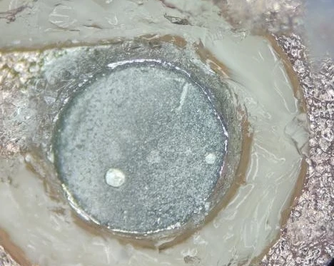
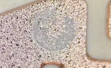
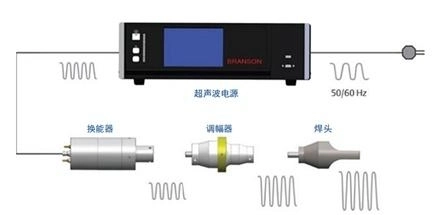
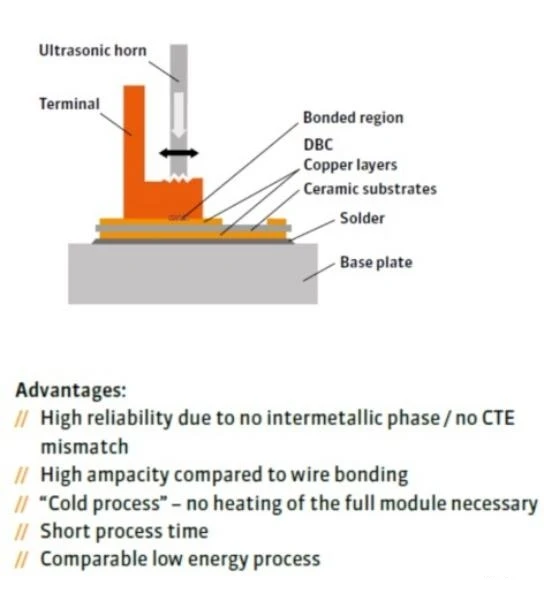
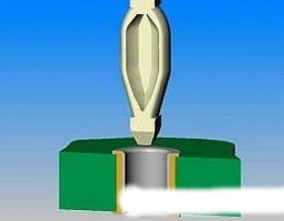
As shown in the figure below is the principle of ultrasonic welding (Ultrasonic Welding). The ultrasonic wire bonding system is mainly composed of a welding head, an amplitude modulator, a transducer and an ultrasonic power supply. This can ultimately transform the power frequency signal of the ultrasonic power supply into high-frequency ultrasonic mechanical vibrations of 20-60 KHz. The wedge applies pressure and ultrasonic energy to the surface of the Pin needle during the ultrasonic welding process. The oxide film between the Pin needle and the DBC is broken by high-frequency vibration friction under their combined action. This process exposes a clean interface. Pressure and ultrasonic energy continue to be applied after the clean copper surface metal makes contact. This process gradually increases the welding contact area. This further causes atoms between the metal surfaces to form covalent bonds. Therefore, a reliable connection is ultimately created.
Advantages of Ultrasonic Pin Welding
- High welding precision and low energy consumption.
- High Units Per Hour (UPH) and short welding time.
- Monitor the quality of the welding process in real-time (deformation, voltage, current, etc.).
- No use of solder or flux during welding, no harm to health.
- Direct surface-to-surface bonding during welding to eliminate the need for filler materials.
- Excellent physical properties, no thermal stress on the product.
- No risk of product oxidation during the operation process, no heating is required
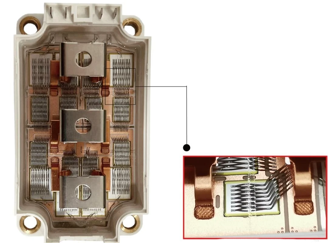
Automated packaging helps achieve encapsulation automation by the pin automatic feeding function. Meanwhile, precise identification, with higher precision than traditional solder paste welding, is conducted before welding, and the process is similar to power terminal ultrasonic welding. The ultrasonic Pin welding technology applied in power module packaging replaces the traditional solder paste brazing process through ultrasonic welding of signal terminals, thereby enhancing the connectivity between Pins and DBC.
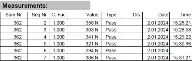
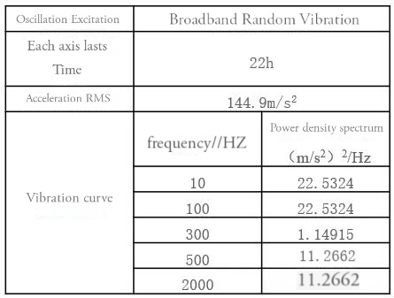
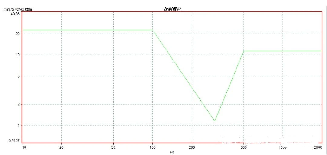
Stable Bonding Surface Thrust
To study the ability of the ultrasonic pin welding solution module to resist external random vibrations and the rationality of its structural design, the vibration frequency of the module under random excitation conditions is obtained by tightening the acceleration to 15G in accordance with the AQG – 324 standard.
High-Temperature Solder Sheet Welding Process
The degradation of solder layers can be accelerated by the creep characteristics of alloy solders under temperature effects due to the CTE (coefficient of thermal expansion) differences among different materials.
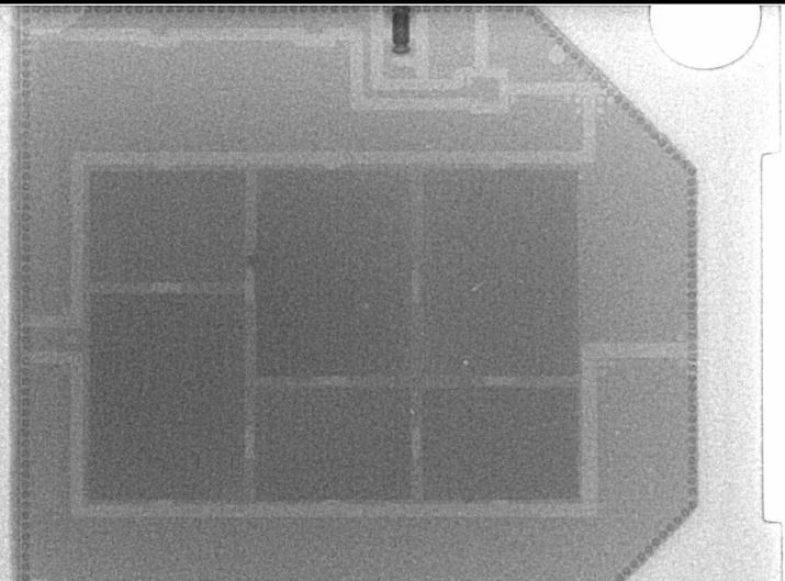
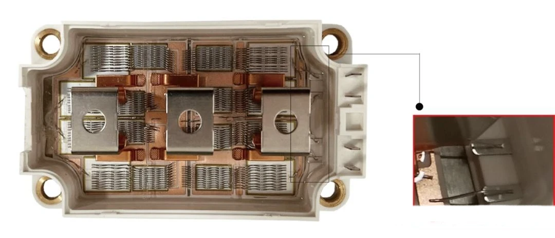
Terminal Ultrasonic Welding
The reliability of the module is improved and parasitic inductance is effectively reduced by applying the ultrasonic welding process to power terminals.
Signal Terminals Made of Copper-clad Aluminum Materials
The bonding strength and the long-term reliability of the module are improved by using copper-clad aluminum materials for signal terminals, as the bonding strength between the aluminum wire and the aluminum surface is higher and the signal terminal connection still adopts the thick aluminum wire bonding technology.
 Symmetrical Design
The consistency of the two bridge arms is ensured and current sharing is effectively achieved by the symmetrical layout of the parallel circuits. Warping of the upper surface during the molding process is avoided by the flat upper surface in the symmetrical design of power terminals, which facilitates user installation and use.
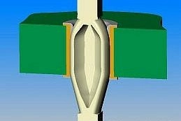
What is PressFIT Technology?
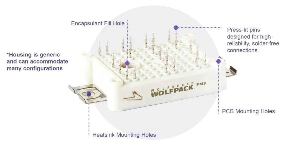
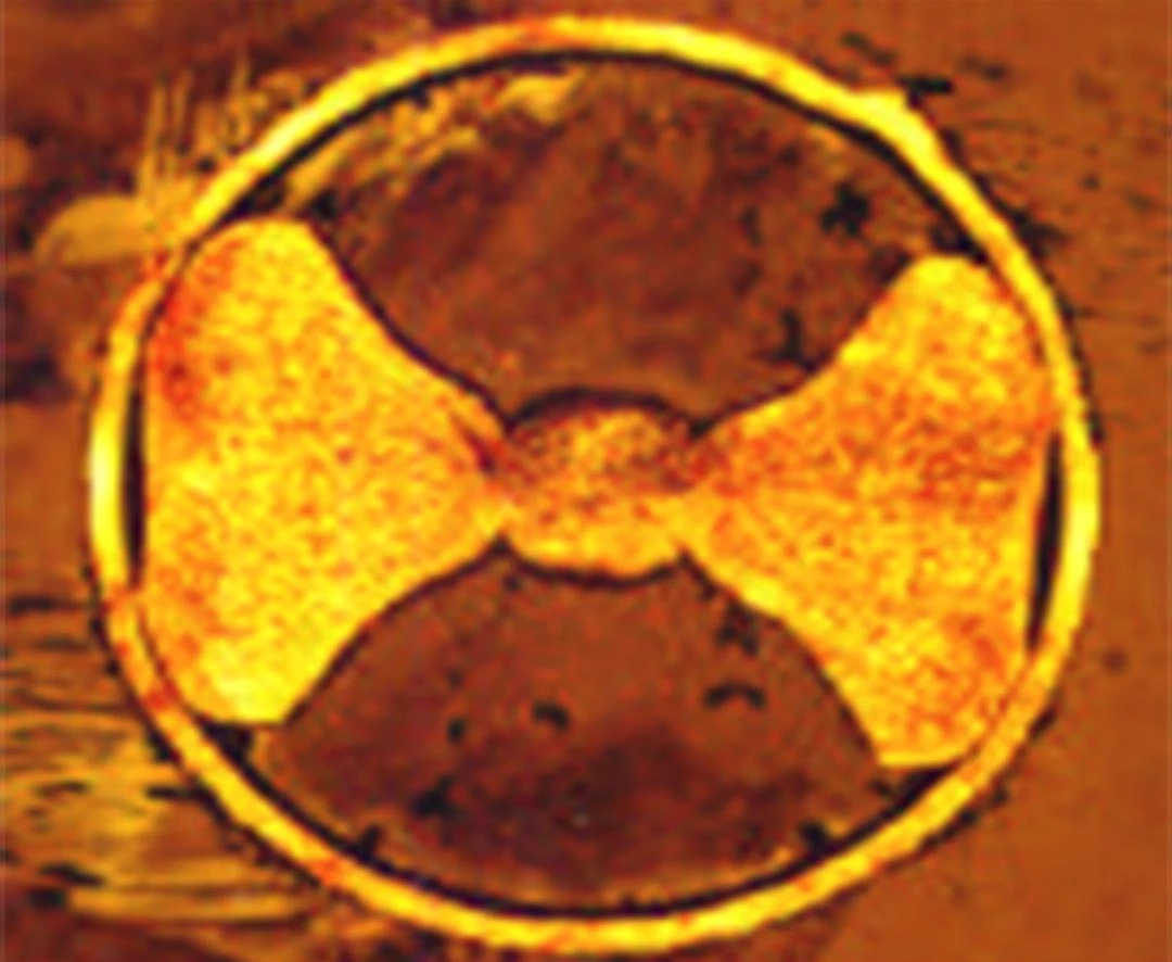
The complete connection method is called PressFIT technology. Pins are secured in PressFIT technology without relying on soldering or any other connection methods. When inserted into appropriately sized and plated PCB through-holes, the pins with a bow-shaped body are compressed, establishing an electrical connection and maintaining mechanical reliability.
Advantage 1: Simplicity
In the new Wolfspeed WolfPACK power module, the module is pushed into place after aligning the pins with the holes on the PCB. Once inserted, the module achieves electrical connection and is mechanically secured. No fastening, special equipment, or multiple operations are required as the design of PressFIT connectors supports simple and efficient installation.
Advantage 2: Higher Power Transmission
Higher current transmission is supported by establishing a secure mechanical connection between the plated through-holes and pins compared with some other connection methods. More outstanding thermal characteristics of PressFIT, including heat dissipation, are presented. Both the enhanced thermal performance and increased current capacity are beneficial for power module applications. Therefore, various converter topologies, such as active rectifiers, buck, and boost circuits, are well-suited for the Wolfspeed WolfPACK power module.
Advantage 3: Low Failure Rate
Applications with high reliability requirements, such as industrial motor drives, grid-connected converters, renewable energy power conversion, are well-suited for the Wolfspeed WolfPACK module because PressFIT is the optimal solution for these scenarios. PressFIT connectors feature one of the lowest failure rates compared to other connection methods: typically, 0.005 FIT (where 1 FIT equal one failure per 10⁹ hours), in stark contrast to screw terminal connections and soldering, which have failure rates as high as 0.5 FIT.
Advantage 4: Prototyping
Fast installation and easy deployment in prototyping are enabled by simply inserting modules using PressFIT pins into a PCB. The modules can be reused in other projects, designs, or configurations due to the removable connections. Although it is easy to install this device, the connections established by PressFIT pins are suitable for use in final products as they are highly reliable.
Advantage 5: PCB Manufacturing
The need for dedicated connectors with potentially long lead times is eliminated in modules, as PressFIT pins do not require specialized components and are directly compatible with PCBs—unlike some connections. A significant advantage of PressFIT pins thus lies in their compatibility with plated through-holes.
Installation time is reduced as PressFIT pins only require the module to be correctly oriented toward the PCB and pushed into place. Overall system costs are reduced by compatibility with plated through-holes in PCBs, as no additional components or assembly steps are required beyond the holes created during PCB manufacturing. Reliability is enhanced by PressFIT pins because modules can only be successfully inserted when correctly oriented, beyond the reduction in installation time and costs.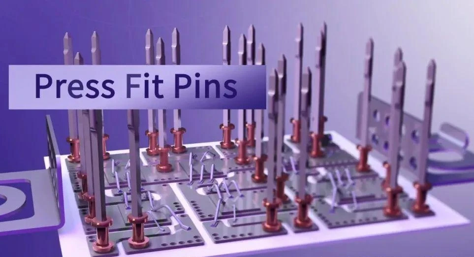
Press-Fit Technology
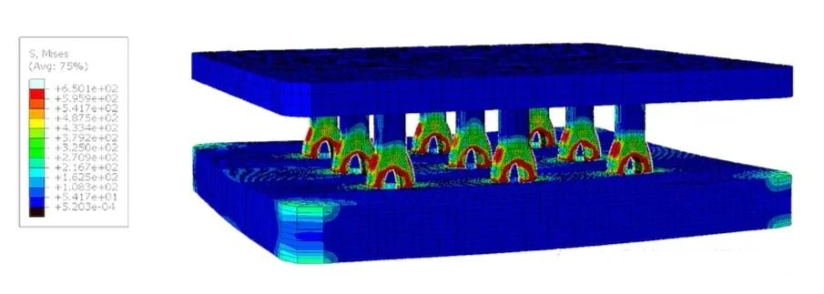
A connection formed by the combination of elastically deformable pins or rigid pins with PCB metallized holes is called Press-Fit press connection technology. Electrical interconnection is achieved through mechanical bonding by creating tight contact points between the pins and metallized holes. Deformation of either the pin cross-section or the metallized holes occur during the press-fit process because the cross-sectional size of the pins must be larger than the diameter of the PCB metallized holes to form a tight fit.
Mechanical electrical conduction and maintenance without the use of soldering technology are enabled by Press-fit, a solderless pin connection technology that allows assembly terminals to connect with printed circuit board (PCB) electroplated through-holes. Various test requirements for automotive electronics (based on international standards such as IEC, EIA, and SAE), including vibration, mechanical performance, and thermal shock (up to 125°C) tests, can be met by its design and testing.
No conductive substances such as flux residues or tin beads that could affect reliable connections;
Elimination of common soldering issues like cold soldering, short circuits, and poor tin penetration;
No need for screws to fix the connector to the PCB after press-fitting;
When using long-pin connectors for press-fitting, the pins extending from the back of the PCB can serve as backside pins to achieve double-sided connections;
Deterministic contact impedance and good high-frequency performance;
High press-fitting efficiency and low cost;
Reusable for assembly (up to three times);
No cleaning required after press-fitting, reducing costs while being environmentally safe;
History of Press-Fit Press Connection
- 1970: Rigid press-fitting
- 1974: C-press and Eye of the Needle flexible press-fitting
- 1983: Tcom press-fit section flexible press-fitting
- 1980s: Application in the communications industry
- 1990s: Application in both the communications and automotive industries
- 2000s: Extensive application in communications, automotive, locomotive, and military industries.
The following types of structures are used for the press-fitting zone by different manufacturers:
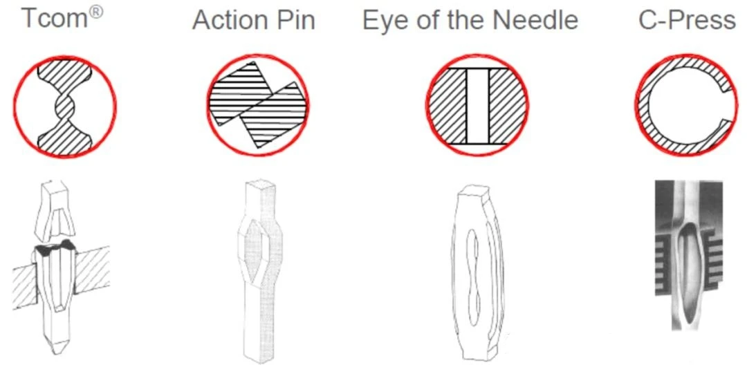
The following standards can be referenced for general design requirements of printed circuit boards. For different brands, varying technical specifications such as press-in force and retention force are determined by the structural design, dimensions, and materials of Pin pins:
- With a hole copper thickness exceeding 25μm and a peel strength of not less than 120N, the metallized hole plating must be uniform and free of burrs.
- The spacing between components and connectors shall be greater than 5mm.
- The maximum width shall be 400 mm.
- The general requirement for hole diameter accuracy is ±0.05mm.
Press-In Force and Retention Force
- The effective press-in force for each pin is preferably not to exceed 150N.
- The minimum retention force requirements for connector pins are specified by German industrial standard DIN 41611.
| Contact Length or Diameter | Minimum Retention Force |
| ≤1.3mm | 30N |
| >1.3mm | 40N |
Materials for Press-Fit
CuSn4/C511, CuSn6/C519, CuSn8/C521
CuCrZr Alloys: C18150/C18160, C18400
Advantages: Moderate strength, stress relaxation performance up to 175°C/1000h, High electrical conductivity
Disadvantages: Formability and plating performance
CuNiSi Alloys: C7025, C19005/C19010
Advantages: Moderate electrical conductivity, high strength, stress relaxation performance up to 150°C/1000h,
Disadvantages: Higher Young’s modulus (direction-dependent on loading)
CuCrZr:C18150/C18160, C18400
Bronze: CuSn4/C511, CuSn6/C519, CuSn8/C521
Advantages: Low Young’s modulus, fine grain structure, high strength level,
Disadvantages: Poor stress relaxation performance under high temperatures (>100°C), low electrical conductivity,
Materials for Press-Fit Applications Meeting the Needs of “Low Temperature Rise, High Current, Miniaturization” Connections
CuNiSi alloys are an ideal choice for miniaturized and signal-intensive connections as improving insertion and extraction forces in Press-Fit connections through special processes can enhance contact stability. They solve the problem of reliable contact in crimped terminals and meet the material requirements for terminals in automotive electronic control units by effectively enhancing contact stability through improved insertion and extraction forces of Press-Fit connections via special processing techniques. Additionally, with the material’s electrical conductivity ranging from 35-60% IACS, low-latency signal transmission is ensured. Their tensile strength exceeds 850% IACS*, guaranteeing reliable connections. CuNiSi alloys deliver excellent comprehensive performance by achieving process breakthroughs through cold working and solution aging strengthening heat treatment.
 The electroplated through-hole copper thickness (PTH Cu thickness) should not be less than 1 mil (average or single point), which is the rule to be followed. It is not allowed to only require the post-plating hole diameter; instead, the drilling size and the post-plating size must be clearly informed to the PCB manufacturer with reference to the component recommended values. Usually, the thickness of copper plating is about 30-55 μm, and the thickness of immersion tin is generally greater than 1 μm. The hole diameter of PTH is generally strictly required, which is specifically determined according to the pin design. The structure of PTH is relatively simple. Generally, the number of PCB layers is more than 4. The plating is generally immersion tin or OSP. The commonly used materials for PTH are fiberglass + epoxy resin + copper foil, with a thickness greater than 1.6 mm. Pins have diverse structures, with the ultimate goal of manufacturing pins that require low press-in force yet offer high retention force under conditions of ease of manufacturing and low cost.
High reliability, superior electrical and thermal performance, and straightforward installation are among the multiple benefits that PressFIT technology delivers to power electronics systems. Simplifying prototyping, modifications, and module replacement, PressFIT pins eliminate the need for soldering, wrenches, and special tools thanks to their reusability. Additionally, the use of plated through-holes in PCBs facilitates the integration of PressFIT pins into designs, while mechanically compressed pins ensure secure connections.
Continue Reading
How to Analysis Terminal Material and Welding Process?
How Many Types of Electrical Terminals and Connector?(Guide for 14 Types)
Connection Methods and Analysis of Terminals and Connectors(5 Necessary Steps)
How many types of connector and terminal insulation materials(3 major categories)
What factors determine the cost of electrical terminals and connectors? (10 Key Factors)
What Certifications Do Terminals and Connectors Need? (6 Common Types)
Connector VS Plug-and-Socket Connector VS Terminal Block, What are they different?